PCB Trace Width and Clearance Rules Expl...

PCB Trace Width and Clearance Rules Explained
Two of the most basic PCB layout decisions are how wide a trace should be and how far it should sit from its neighbors. They look like simple design-rule entries, but they affect whether a board runs cool, survives high voltage, can be built at a sensible cost, and works at high speed. This guide covers the theory, the standard-based formulas, worked examples, and a checklist. Where a number comes from a specific standard, we say so. Where something is a rule of thumb, we label it that way.
PCB Trace Width and Clearance Rules Explained
A practical guide from the engineers at Mekatron Systems Pvt. Ltd.
Two of the most basic PCB layout decisions are how wide a trace should be and how far it should sit from its neighbors. They look like simple design-rule entries, but they affect whether a board runs cool, survives high voltage, can be built at a sensible cost, and works at high speed.
This guide covers the theory, the standard-based formulas, worked examples, and a checklist. Where a number comes from a specific standard, we say so. Where something is a rule of thumb, we label it that way.
A note on standards: IPC and IEC documents are revised periodically. Values here are for orientation. Always check the current revision of the standard that applies to your product before finalizing a design.
1. Why Trace Width and Clearance Matter
Concern | What it governs | Primary driver |
|---|---|---|
Current-carrying capacity | Heating of the conductor | Trace width × copper thickness |
Voltage isolation | Arcing, tracking, breakdown between conductors | Clearance and creepage |
Manufacturability | Yield, cost, reliability of the fabricated board | Fab capability vs. your minimum width/spacing |
Signal integrity | Impedance, crosstalk, reflections | Trace geometry relative to the reference plane and dielectric |
Width and clearance are separate decisions. Width is set mainly by current. Clearance is set mainly by voltage. A 10 A trace at 5 V needs wide copper but little gap. A 10 mA trace at 400 V can be thin but needs millimetres of space. A net that carries both high current and high voltage needs both, and they compete for the same board area.
2. Key Terminology
Term | Meaning |
|---|---|
Trace (track) width | Width of the copper conductor in the plane of the board |
Copper thickness | Thickness of the copper layer, usually quoted as weight in oz/ft² |
Clearance | Shortest distance through air between two conductive parts |
Creepage | Shortest distance along the surface of the insulating material between two conductive parts |
Spacing | General term for the gap between conductors; in IPC-2221 it is the electrical conductor spacing |
Temperature rise (ΔT) | Increase of conductor temperature above ambient due to I²R heating |
Working voltage | Highest voltage across the insulation in normal operation (peak or RMS, depending on the standard) |
Copper weight to thickness
"1 oz copper" means one ounce of copper spread evenly over one square foot.
Copper weight | Thickness (µm, approx.) | Thickness (mil, approx.) |
|---|---|---|
½ oz/ft² | 17.5 | 0.69 |
1 oz/ft² | 35 | 1.37 |
2 oz/ft² | 70 | 2.74 |
3 oz/ft² | 105 | 4.11 |
Unit conversion: 1 mil = 0.001 inch = 25.4 µm. Finished outer-layer copper is usually somewhat thicker than the base foil because of plating, so check your fabricator's finished-copper specification.
Clearance vs. creepage
On a flat board with nothing in between, both distances are the same. They differ when there is a slot, rib or barrier. A milled slot between primary and secondary on a mains board barely changes the air clearance but greatly lengthens the surface (creepage) path. This is why isolation slots are common on mains-powered boards.
3. Current-Carrying Capacity
3.1 What affects ampacity?
- Cross-sectional area. Wider and thicker copper gives lower resistance and less heating.
- Allowed temperature rise. A 10 °C rise is a conservative choice. 20 to 30°C is common where the board and enclosure can tolerate it.
- External vs. internal layers. Outer traces shed heat to the air by convection and radiation. Inner traces are buried in laminate and, in the IPC-2221 model, need roughly twice the width for the same current.
- Surroundings. Nearby copper planes, thermal vias, board thickness, laminate conductivity, and airflow all change real-world heating.
- Duty cycle. For short pulses, thermal mass lets a trace carry more than its continuous rating. Check fusing and melting limits separately.
3.2 The IPC-2221 approach
IPC-2221 (Generic Standard on Printed Board Design) gives trace-width curves from which the following widely used fitted equation is derived:
$$ I = k \cdot \Delta T^{0.44} \cdot A^{0.725} $$
where:
- $$ I $$ = maximum current in amperes
- $$ \Delta T $$ = temperature rise above ambient in °C
- $$ A $$ = cross-sectional area in square mils (width in mil × thickness in mil)
- $$ k = 0.048 $$ for external layers
- $$ k = 0.024 $$ for internal layers
Rearranged to find the required cross-section:
$$ A = \left(\frac{I}{k \cdot \Delta T^{0.44}}\right)^{1/0.725} \qquad \text{Width (mil)} = \frac{A}{\text{thickness (mil)}} $$
Limitations. The IPC-2221 curves come from old test data on a small set of board configurations. They are generally regarded as conservative for external traces and less reliable for internal traces and for boards with planes nearby. The equation is only a curve fit and should not be extrapolated far outside the original data range.
3.3 The IPC-2152 approach
IPC-2152 (Standard for Determining Current-Carrying Capacity in Printed Board Design) replaced the older IPC-2221 charts with newer test data. In short:
- It provides a baseline set of conservative charts and also shows how the result changes with real board conditions.
- It recognizes that the thermal conductivity of the board materials, vias, copper planes, power dissipation, and board thickness all affect how much current a trace can carry, as the IPC product description states.
- It showed that the old assumption that internal traces run hotter than external ones is not generally true. Internal traces can have comparable or better performance because heat spreads through the laminate.
- It does not reduce to one simple closed-form equation like IPC-2221. It is presented as charts and correction guidance, so many designers use IPC-2152-based calculators or thermal simulation.
Aspect | IPC-2221 | IPC-2152 |
|---|---|---|
Form | Curves, with a popular curve-fit equation | Charts plus correction factors and guidance |
Internal vs. external | Internal needs about 2× width in the fit (k = 0.024 vs 0.048) | Treats the difference as much less clear-cut |
Effect of planes, vias, and board thickness | Not modelled | Addressed |
Typical outcome | Conservative, simple | More realistic when conditions are known |
Practical rule: use IPC-2221 for a quick, safe first estimate. Use IPC-2152 methods when the board is tight on space or runs hot, or the design is safety-critical, and verify with a prototype temperature measurement.
3.4 Worked example: 3 A on an outer layer
Given: 3 A, 1 oz copper (1.37 mil), external layer, ΔT = 10°C.

Result: about 54 mil (≈1.4 mm) for 3 A at a 10°C rise on 1 oz external copper, by the IPC-2221 fit.
Same current on an internal layer: k = 0.024 halves the allowed current for a given area. The required area becomes 2^{1.379} \approx 2.6 times larger, so the width is about 142 mil (≈3.6 mm). Under IPC-2152, this penalty is often smaller in practice.
Allowing a 30°C rise (external): 30^{0.44} \approx 4.47, so k . ΔT^{0.44} \approx 0.2146 and A = (3/0.2146)^{1.379} \approx 38.2 { mil}^2. The width is about 28 mil (≈0.7 mm).
Doubling copper to 2 oz (2.74 mil) halves the width needed for the same area, so the 10 °C external case drops to roughly 27 mil.
Always add margin. Round up, then check how much copper your layout allows. Remember that vias, narrow necks at pads and connectors, and the current's return path are often where heating actually occurs.
4. Voltage Clearance and Creepage
4.1 What drives the required spacing
Factor | Effect |
|---|---|
Working voltage | Higher voltage needs larger clearance and creepage. Use peak voltage for clearance. 230 V RMS mains peaks near 325 V. |
Pollution degree | Dust, moisture, and conductive contamination increase risk. IEC 60664-1 defines pollution degrees 1 to 4. A higher degree means larger required distances, mainly for creepage. |
Material group (CTI) | The Comparative Tracking Index measures resistance to surface tracking. IEC 60664-1 classifies materials into groups I, II, IIIa and IIIb. A lower group number (higher CTI) allows shorter creepage. Standard FR-4 is commonly in the middle groups, but check the laminate datasheet. |
Altitude | Thinner air at altitude lowers the breakdown voltage of air, so clearances need correction factors above 2000 m. |
Insulation type | Functional, basic, supplementary, and reinforced insulation need progressively more. Reinforced insulation, as used between mains and user-accessible circuits, is the most demanding. |
Overvoltage category and transients | Mains transients set the required impulse withstand voltage, which sets clearance. |
Coating | A permanent conformal coating or solder mask can reduce external spacing in IPC-2221. Safety standards treat coatings more cautiously. |
4.2 IPC-2221 Table 6-1: Electrical conductor spacing
IPC-2221 Table 6-1 gives minimum spacing by peak voltage between conductors. The values below are from IPC-2221 Table 6-1, converted to millimetres. Columns B1, B2 and B4 are for internal conductors, external uncoated conductors (sea level up to 3050 m), and external conductors with permanent polymer coating, respectively.
Voltage between conductors (DC or AC peak) | B1: Internal | B2: External, uncoated | B4: External, with coating |
|---|---|---|---|
0 to 15 V | 0.05 mm | 0.1 mm | 0.05 mm |
16 to 30 V | 0.05 mm | 0.1 mm | 0.05 mm |
31 to 50 V | 0.1 mm | 0.6 mm | 0.13 mm |
51 to 100 V | 0.1 mm | 0.6 mm | 0.13 mm |
101 to 150 V | 0.2 mm | 0.6 mm | 0.4 mm |
151 to 170 V | 0.2 mm | 1.25 mm | 0.4 mm |
171 to 250 V | 0.2 mm | 1.25 mm | 0.4 mm |
251 to 300 V | 0.2 mm | 1.25 mm | 0.4 mm |
301 to 500 V | 0.25 mm | 2.5 mm | 0.8 mm |
Above 500 V (add per volt) | +0.0025 mm/V | +0.005 mm/V | +0.00305 mm/V |
For voltages above 500 V, the per-volt figure is added to the 500 V value. For example, an uncoated external gap at 1000 V is 2.5 + 500 X 0.005 = 5.0 mm.
IPC-2221 also has columns B3 (external, uncoated, above 3050 m altitude) and A5 (component leads with conformal coating), which are not reproduced here. Consult the standard directly if you design for high altitude.
4.3 Worked example: 230 V AC mains, uncoated outer layer
- Peak voltage = 230 \times \sqrt{2} \approx 325 V.
- 325 V falls in the 301 to 500 V row.
- IPC-2221 B2 (uncoated external): 2.5 mm. With a permanent coating (B4): 0.8 mm.
Using the RMS figure of 230 V would wrongly place you in the 171 to 250 V row (1.25 mm), and that is one of the most common errors with this table. Also note that the voltage that matters is the difference between the two conductors at the gap, not the highest rail on the board.
4.4 Safety standards come first
IPC-2221 is a general board-design standard. It is not a product-safety standard. For mains-connected or safety-critical equipment, the applicable product standard sets the requirements. These standards usually draw on IEC 60664-1 (Insulation coordination for equipment within low-voltage supply systems), and typical product standards include IEC/EN 62368-1 for audio/video and ICT equipment, IEC 61010-1 for measurement and control equipment, and IEC 60335-1 for household appliances. In these:
- Clearance is determined from the required impulse withstand voltage and pollution degree.
- Creepage is determined from working RMS voltage, pollution degree and material group.
- The result is often larger than IPC-2221 and must be met in addition to it.
We deliberately do not give a generic creepage table here. The right value depends on the product standard, insulation class, pollution degree, CTI group and altitude. Look it up in the current edition of the standard that applies to your product, or get advice from a certified test house.
4.5 Practical techniques for high-voltage boards
- Mill isolation slots to increase creepage between primary and secondary.
- Keep solder-mask openings and exposed copper away from high-voltage gaps.
- Round pad and trace corners. Sharp points concentrate electric fields.
- Apply conformal coating where the standard allows it, and verify coverage.
- Keep the creepage path clean. Flux residue and contamination reduce effective isolation.
5. Manufacturing Constraints
Your design has to be buildable by your fabricator, at an acceptable cost and yield.
5.1 Why minimums exist
Etching removes copper from the sides of every trace, a process called undercut. Thicker copper takes longer to etch, so it needs wider minimum traces and spacing. Registration tolerance, drill wander and solder-mask alignment add further limits.
5.2 Typical capability
Capabilities vary between fabricators and change with technology level, so we deliberately give no single universal numbers. As a general pattern:
Copper weight | Relative minimum trace/space |
|---|---|
½ oz | Finest |
1 oz | Standard |
2 oz and above | Noticeably coarser |
Ask your fabricator for its current design rules, including minimum trace/space, annular ring, drill size, copper-to-edge distance and solder-mask dam width.
5.3 Effect on cost and yield
- Tighter than standard rules means more rejects, slower processes and a higher price.
- Using the finest geometry everywhere is a common cost mistake. Use fine geometry only where needed, such as under fine-pitch BGAs, and relax it elsewhere.
- Heavy copper needs wider spacing and may need special process steps.
- Wider spacing improves yield, and also helps reliability by reducing short-circuit and dendrite risk.
Rule of thumb: design to the fabricator's standard capability, not its advanced capability, unless the design requires otherwise.
6. High-Speed and Signal Integrity Considerations
6.1 Controlled impedance
At high edge rates a trace behaves as a transmission line. Its characteristic impedance Z_0 depends on:
- trace width (wider gives lower Z_0)
- copper thickness (thicker gives slightly lower $$ Z_0 $$)
- dielectric height to the reference plane (greater height gives higher $$ Z_0 $$)
- dielectric constant $$ \varepsilon_r $$ (higher gives lower $$ Z_0 $$)
An older, widely quoted approximation for surface microstrip is:
$$ Z_0 \approx \frac{87}{\sqrt{\varepsilon_r + 1.41}} \ln!\left(\frac{5.98,h}{0.8,w + t}\right) $$
where $$ h $$ is dielectric height, $$ w $$ is trace width and $$ t $$ is copper thickness (same units), and the formula is generally quoted as valid for roughly $$ 0.1 < w/h < 2.0 $$ and $$ 1 < \varepsilon_r < 15 $$. It is an approximation. For production designs, use your fabricator's field-solver stackup data, because the actual $$ \varepsilon_r $$, prepreg thickness and etch profile change the result.
Common targets are 50 Ω single-ended and 90 to 100 Ω differential, depending on the interface standard (USB, HDMI, Ethernet and others). Follow the interface specification.
6.2 Spacing and crosstalk
- Crosstalk falls as the gap between parallel traces grows relative to the height above the reference plane.
- The 3W rule (centre-to-centre spacing of three times the trace width) is a rule of thumb that reduces coupling. It is not a guarantee, and critical signals may need more.
- Keep a continuous reference plane under high-speed traces, and avoid routing across plane splits.
- For differential pairs, keep the gap and width constant along the route and match lengths as the interface requires.
6.3 Interaction with power rules
Trace width chosen for current may not match the width needed for impedance. Use the width needed for each purpose on the respective net, and do not apply one global width to the whole board.
7. Common Design Mistakes and How to Avoid Them
Mistake | Why it hurts | How to avoid it |
|---|---|---|
Using RMS instead of peak voltage for clearance | Under-sized gaps on mains designs | Convert to peak; check the product standard |
Using one design rule for the whole board | Wasted area, or unsafe gaps at high voltage | Define net classes with different width and clearance |
Sizing width from current alone and ignoring ΔT | Hot boards, early failure | Choose ΔT deliberately; verify with a prototype |
Narrow necks at pads, vias and connectors | Local hot spots | Check the narrowest point on the current path |
Too few vias on high-current layer changes | Via overheating | Use several vias in parallel |
Assuming solder mask replaces proper clearance | Mask can be damaged or opened | Keep air clearance wherever the standard requires |
Ignoring creepage | Surface tracking, failed safety tests | Use slots; follow the product standard |
Specifying finest geometry everywhere | Higher cost, lower yield | Use fine rules only where needed |
Not checking the fabricator's rules | DFM holds, redesign | Get design rules before layout |
Impedance rules without stackup confirmation | Mismatched impedance | Agree the stackup with the fabricator early |
Sharp 90° corners on HV traces | Field concentration | Use rounded or 45° corners |
8. Practical Design Guidelines
- Start from requirements. List maximum current, ΔT limit, working and peak voltages, applicable safety standards, environment (pollution, altitude), and impedance targets.
- Set net classes for power, high voltage, high speed and general signal nets.
- Size power traces with an IPC-2221 estimate, refine with IPC-2152 methods if needed, and add margin.
- Use planes or copper pours for high-current paths where possible, since wider copper shares heat.
- Set clearances from the product standard first. Use IPC-2221 as a general baseline where no specific standard applies.
- Add isolation slots and keep-outs at mains barriers.
- Agree the stackup with your fabricator for controlled-impedance boards.
- Run DRC with real values, then review the high-voltage and high-current areas by eye.
- Prototype and measure. Check temperature rise under load, and perform the relevant safety tests such as hipot.
9. Summary Checklist
Current
- Maximum and continuous current per net defined
- ΔT limit chosen
- Width calculated (IPC-2221 or IPC-2152) with margin
- Internal vs. external layer accounted for
- Narrowest point on the path checked (pads, vias, connectors)
- Via count adequate for current
Voltage
- Peak working voltage between each pair of conductors identified
- Applicable safety standard identified (IEC 60664-1 based product standard)
- Pollution degree, material group (CTI), altitude and insulation type considered
- Clearance and creepage both verified
- Isolation slots or keep-outs in place where needed
Manufacturing
- Fabricator design rules obtained
- Minimum trace/space suited to copper weight
- Fine geometry limited to areas that need it
Signal integrity
- Impedance targets and stackup agreed
- Continuous reference planes
- Crosstalk spacing reviewed
Verification
- DRC run with correct net-class rules
- Prototype thermal test done
- Safety testing planned
Conclusion
Trace width comes mainly from current and acceptable temperature rise. Clearance and creepage come mainly from voltage, environment and the applicable safety standard. Both must also fit within what your fabricator can build reliably and, on fast boards, within controlled-impedance geometry. Treat IPC-2221 as a good general starting point. Use IPC-2152 for more realistic thermal results, and defer to IEC 60664-1-based product standards for any safety-critical or mains-connected design.
Work with Mekatron. Mekatron Systems Pvt. Ltd. designs and manufactures PCBs and provides PCB assembly from our base in Kolkata. Whether you need a design review of your trace-width and clearance rules, a quote for prototype or volume boards, or assembly support, our team is ready to help. Visit www.mekatron.in to get in touch.
Standards referenced
- IPC-2221 – Generic Standard on Printed Board Design (including Table 6-1, Electrical Conductor Spacing, and the trace-width curves behind the I = k·ΔT^0.44·A^0.725 fit)
- IPC-2152 – Standard for Determining Current-Carrying Capacity in Printed Board Design
- IEC 60664-1 – Insulation coordination for equipment within low-voltage supply systems
- IPC-2141 – Controlled Impedance Circuit Boards and High-Speed Logic Design (source of the classic microstrip approximation)
Disclaimer: This article is for general educational guidance and does not replace the text of the standards or professional safety certification. Verify all values against the current standard revision before use.
Verification notes for your editor: The IPC-2221 constants (k = 0.048/0.024, exponents 0.44 and 0.725) and the Table 6-1 values were confirmed from multiple sources during research. The IPC-2152 points are consistent with IPC's own description, but I couldn't access the full standard, so please check them against your copy. The microstrip formula and the IEC 60664-1 group and degree descriptions are standard textbook material that I did not re-verify online. Please confirm them against your copy of the standards before publishing. I deliberately left out generic creepage tables and fabricator minimum trace/space numbers, since those depend on the applicable standard and on your own process capability.
Our Products
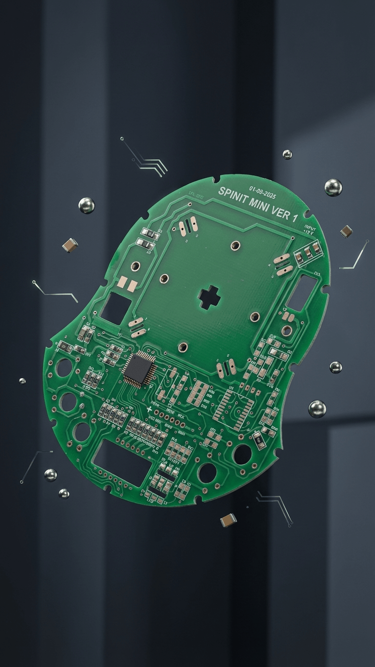
PTH Double Sided PCB
Plated Through Hole (PTH) double-sided PCBs offering higher circuit density, strong mechanical bonding, and enhanced reliability.
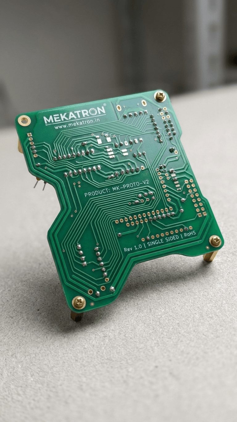
Single Sided PCB
Reliable single-layer printed circuit boards ideal for simple electronic applications and power supplies.
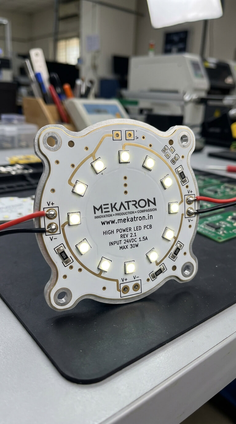
Aluminum Metal Core PCB
Metal Core PCBs specially designed for LED applications, ensuring excellent heat dissipation and longer product life.